Mavericks femtosecond Cr:Forsterite laser Specifications
Model Mavericks 65P
Pulse duration, fs < 70
Tuning range, nm 1230-1270
Output power, mW* 180-250
Recommended pump power, W 6-10
Repetition rate, MHz 75/100/125
Output stability, rms < 2%
Spatial mode TEMoo
Polarization, Linear horizontal
Divergence, mrad < 2
Crystal cooling thermoelectric
* - depends on the pump power and operating temperature
The electro-magnetic mode-lock starter provides mode-locking regime. This
model has integrated fiber pump laser. |
 |
Featured application
High Resolution Impedance and Potential Imaging using a
Mavericks Cr:Forsterite Laser
Steffi Krause, Department of Materials, Queen Mary University of London, London
E1 4NS
Photocurrent measurements at field-effect structures such as
electrolyte-insulator-semiconductor or metal-insulator-semiconductor structures
have been used to measure local electrical potentials, local concentrations such
as pH or hydrogen and the local impedance of thin films (Figure 1) [1,2]. Local
concentration and potential measurements are known as Light Addressable
Potentiometric Sensors while local impedance measurements are carried out using
Scanning Photo-induced Impedance Microscopy. In both techniques electron-hole
pairs are generated by a laser focused into the space charge region of the
semiconductor. If the field-effect structure is biased towards depletion or
inversion the photo-generated charge carriers separate in the field of the space
charge region causing a current to flow. Modulation of the laser beam intensity
results in an ac-photocurrent. As the current is limited to the illuminated area
of the structure measurement can be carried out with spatial resolution.
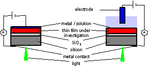
Figure 1. Field-effect structures used for local impedance and potential
measurements.
The dependence of the photocurrent on the dc voltage applied is shown in
Figure 2. With increasing depletion an increase in the photocurrent is observed
reaching a plateau when the structure is biased towards inversion. A shift of
the photocurrent curve along the voltage axis indicates a change in the local
potential; a change in the maximum photocurrent can be translated into a change
in the local impedance of materials deposited onto the insulator. This technique
has potential applications in the characterization of heterogeneous materials or
the local electrical properties of living cells or biological membranes.
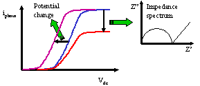
Figure 2. Changes in the maximum photocurrent and the position of the
photocurrent curve on the dc voltage axis can be used to measure local impedance
or electrical potentials
Lateral resolution of photocurrent measurements
The lateral resolution of photocurrent measurements is determined by the
properties of the semiconductor substrate, the quality of the focus of light and
the wavelength employed. Charge carriers generated in the bulk of the
semiconductor substrate do not only diffuse to the space charge layer where they
cause a current but they also diffuse laterally resulting in a loss of
resolution. Recent experiments have shown that the lateral diffusion length of
charge carriers can be reduced to less than one micrometer by using a thin
epitaxial layer of silicon on a sapphire substrate (SOS) or a semiconductor with
a short diffusion length of charge carriers such as amorphous silicon [4].
However in both cases the low quality of the insulator limits the application of
these semiconductor substrates.
To avoid the problems encountered using thin silicon layers and amorphous
silicon, it would be advantageous if bulk silicon could be employed. However, if
a laser beam is focused into the space charge region from the back of the
semiconductor substrate, light has to travel through the bulk of the material
where it generates charge carriers resulting in a loss of resolution (Figure 3).
If light with energy smaller than the bandgap is used, no charge carriers are
generated in the bulk of the semiconductor. Electron-hole pairs are generated
only in the focus near the space charge layer at the semiconductor/insulator
interface due to two-photon absorption. The possibility of high- resolution SPIM/LAPS
measurements using a two-photon effect in bulk silicon will be investigated.
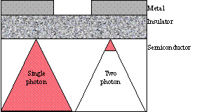
Figure 3. In case of a single photon effect charge carriers are produced
throughout the bulk of the material. In case of a two photon effect charge
carrier generation is confined to the focus near the space charge region of the
semiconductor
References
1. S. Krause, H. Talabani, M. Xu, W. Moritz, and J. Griffiths,
Electrochim. Acta, 47, 2143-2148 (2002).
2. W. Moritz, T. Yoshinobu, F. Finger, S. Krause, et al., Sens. Actuator B-Chem.,
103, 436-441 (2004).
3. S.N. Jayasinghe, M.J. Edirisinghe, D.Z. Wang, Nanotechnology, 15, 1519-1523
(2004)
4. S. Krause, W. Moritz, H. Talabani, M. Xu, A. Sabot, G. Ensell, Electrochim.
Acta, in press
5. E. Ramsay, N. Pleynet, D. Xiao, R. J. Warburton, and D. T. Reid, Opt. Lett.,
30, 26-28 (2005).
Del Mar Photonics